This is default featured slide 1 title

Lorem ipsum dolor sit amet, consectetur adipisicing elit, sed do eiusmod tempor incididunt ut labore et dolore magna aliqua. Ut enim ad minim veniam. blogger theme by BTemplates4u.com.

This is default featured slide 2 title

Lorem ipsum dolor sit amet, consectetur adipisicing elit, sed do eiusmod tempor incididunt ut labore et dolore magna aliqua. Ut enim ad minim veniam. blogger theme by BTemplates4u.com.

This is default featured slide 3 title

Lorem ipsum dolor sit amet, consectetur adipisicing elit, sed do eiusmod tempor incididunt ut labore et dolore magna aliqua. Ut enim ad minim veniam. blogger theme by BTemplates4u.com.

This is default featured slide 4 title

Lorem ipsum dolor sit amet, consectetur adipisicing elit, sed do eiusmod tempor incididunt ut labore et dolore magna aliqua. Ut enim ad minim veniam. blogger theme by BTemplates4u.com.

This is default featured slide 5 title

Lorem ipsum dolor sit amet, consectetur adipisicing elit, sed do eiusmod tempor incididunt ut labore et dolore magna aliqua. Ut enim ad minim veniam. blogger theme by BTemplates4u.com.

Friday 3 May 2013

LITER OF LIGHT


We dream about tomorrow’s glowing world………...........We are the team of “Liter of Light” in India……..
Mission
spreading this innovation in our country and installing the liter of light in India.
Description
The  source of light consists of a plastic bottle filled with a water solution which is embedded in the roofs of houses. The solar bottle harnesses the light from the sun, capturing and diffracting the light to all parts of the room. Our aim is to support this idea which has already launched in many countries around the world.
 Founded - September 12,2011
Products- A soda bottle as a light source in underprivileged households.


Liter of Light India Abstract :
             We are a group of under graduate students working to install liter of lights or solar blubs all over India.Our motto is to lighten up the most unprivileged communities by installing solar bulbs.Introducing such low-cost technologies we aim to glow about one million homes throughout India.
What is Liter of Light :
              A Liter of Light is a zero-carbon emitting solar lighting project which is first initiated by members of My Shelter Foundation and students of the Massachusetts Institute of Technology.Solar Bottle Bulb uses appropriate technologies that are highly replicable and sustainable. The materials used are found easily in the poorest neighborhood.They can be easily built with simple carpentry skills and little knowledge about the solar bulb. This simple mechanism of installing Solar Bottle Bulb made the expansion of movement easy.
Do it Yourself Liter of Light:
               The bulb is nothing but a A 1.5 liter clear PET bottle which is used as source of light.It is filled with the mixture of water and bleach.The bottle with this mixture is inserted into a metal sheet.This kit is embedded on the roofs of houses which acts as a source of light.
Working principle of Liter of Light :
                Solar Bottle Bulb works by the refraction of light rays.The sun rays falling on the bottle gets refracted when it immediately enters water i.e. due to change in medium form air to water.This refracted light spreads at an angle of 360 degrees in a room and produces light equivalent to 60 watts bulb.
                The solar bulb lasts for 5 years without any sort of maintenance with the change of water at regular intervals.Bleach is added to maintain the clarity of water and make the water free from microorganisms.
 Why Liter of Light :

  • Solar Bottle Bulb does not have any carbon emissions when compared to any conventional light.
  • Solar Bottle Bulb is a source of livelihood for the local unemployed people.
  • It is very economic and reliable.
  • It reduces the impact of global warming on earth.
  • Disposed plastic is up-cycled.
      https://www.facebook.com/pages/Liter-of-Light-in-India/204926342960861 - FOLLOW THIS LINK .

Thursday 2 May 2013

FPGA vs ASIC

FPGA --- Field-Programmable Gate Array
ASIC --- Application-Specified Integrated Circuit
A field-programmable gate array (FPGA) can be purchased off-the-shelf and programmed by the user, whereas an application-specific integrated circuit (ASIC) is manufactured to a customer’s specification. This distinction has not changed since the dawn of both technologies.


Time-to-market and configurability
The configurability of an FPGA is its most priced asset. Its ability to rapidly implement or reprogram the logic for a specific feature, or to modify the functionality that was previously instilled in it, is why designers run after it.


“Even if a vendor has new features to add at a later stage in the released product, he still has the freedom to decide whether to implement that feature in software or hardware based on applicability. Time-to-market for handling change-requests in FPGA is much less than in ASICs,” explains Manisha Mankar, architect—digital design, Robert Bosch Engineering and Business Solutions.

Indeed, this is one of the primary reasons why designers are opting for FPGAs.

“There are two key factors driving the demand for FPGAs today: The programmable imperative, i.e., the inherent capability of an FPGA that allows it to be tailored to the needs of the customer and the insatiable bandwidth requirements of the mobile generation today. Given this, FPGAs are increasingly replacing ASICs and ASSPs for more and more applications across different verticals such as telecommunications, aerospace, medical, automotive and industrial to name a few,” adds Neeraj Varma, director-sales, Xilinx India.


 Performance and power efficiency
While FPGAs used to be selected for lower-speed, less complex or volume designs in the past, today’s FPGAs easily push the performance barrier. With increase in logic density and other features such as embedded processors, DSP blocks and high-speed serial at low price points, FPGAs are an interesting proposition. The industry has shown that high-end FPGAs are growing in volume, handling high-speed applications and complex designs.Earlier, FPGAs were viable only for prototyping or low-density applications. Now they meet the needs of very high-volume applications such as consumer products and other moderate-volume high-density appli-cations as well.
The fact that ASICs are built for specific applications allows them to have a very high density of useful logic gates on the chip and use resources optimally. Hence higher gate count and lower power consumption give ASICs a competitive edge over FPGAs. 

High volume production

For high-volume production, costs associated with building a custom ASIC chip are said to be increasing, especially since technology nowadays is ever more complex. As we move towards advanced nodes, cost considerations multiply exponentially. For instance, the development cost for ASIC at 28nm is 40 per cent more than at 40nm. At 20nm, it is estimated to be 70 per cent over that of 28nm.

Best of both the worlds
While FPGAs are excellent for designing and prototyping digital logic into medium-volume, medium-density applications, their high unit cost makes things difficult. On the other hand, the low unit cost of ASICs is one of the main reasons why these are considered for high-volume manufacturing.

What if there were a way to get the best of both the worlds? Well, designing a new product around FPGA allows design modifications to be quickly made throughout the development process. Once this design is complete and approved for production, the FPGA design can be migrated to an ASIC design and then produced, cutting the production unit cost greatly.


LEDs for Solid-state Lighting

Solid-state electronics has been transforming our lives for many decades by bringing us increasingly small, cheap and efficient devices and appliances. Our modern life-styles have come to be defined by our access to an increasingly wide assortment of technologically advanced equipment for personal and group use. From smart phones to personal music players and from satellite navigators to tablet computers the benefits of modern electronics are all around us. In this continuing tradition, solid-state lighting now seems set to revolutionise the way we light our surroundings - indoors and outdoors. Its impact is already being felt globally and in the coming years it will further entrench its position as one of the defining technologies of the twenty-first century. 


Lighting technology has changed remarkably little since its inception more than a hundred years ago. We still illuminate our homes and offices with lamps that bear a striking resemblance to Thomas Edison’s invention in the late nineteenth century. Indeed the basic design of incandescent light bulbs has remained essentially the same over the years and with that their efficiencies have also changed very little. The development of tungsten-halogen lamps in the nineteen-fifties did raise the efficiency somewhat but it still remained woefully low. The later development of fluorescent lighting resulted in a big improvement in efficiency but even that is now considered insufficient in our increasingly energy-conscious world. Moreover, their use of toxic and environmentally hazardous mercury has always remained a cause for concern. The emergence of highly efficient diode-based solid-state lighting over the past decade has, therefore, been widely welcomed and acknowledged as the next logical step in the evolution of lighting technology.

Solid-state light emitters were invented in the nineteen sixties as semiconductor pn-junction diodes capable of emitting coloured light. These light-emitting diodes (LEDs) were made from materials such as gallium arsenide and gallium arsenide phosphide. For many years, LEDs only served as small indicator lights for electronic equipment. They were ubiquitous in everything from portable transistor radios to televisions and telephones. Epoxy-packaged low-power LEDs are still around in essentially the same form in which these devices have been used for several decades.  In later years, LEDs were also used to build dot-matrix displays that found particular favour in countries of the far-east. Even today a visitor to such places as Hong Kong, Singapore or Tokyo cannot escape the overwhelming concentration of advertising LED bill boards in city centres. Traffic light is another application where LEDs made an early appearance.

A typical LED-based traffic light utilising clusters of low-power red, amber and green LEDs is shown in figure.

LEDs were traditionally available in most colours except blue which made it impossible to build full-colour displays using a combination of red, green and blue light emitters. A blue-emitting LED was a long sought after goal and, therefore, it caused much excitement when a practical blue LED was reported by a researcher at a small Japanese electronics company. Following figure  shows an LED wafer with many individual blue LEDs, undergoing testing on an assembly line. Shuji Nakamura’s invention of the blue LED at Nichia Corporation resulted in the proliferation of LEDs in all kinds of applications. Its development also gave rise to the white LED which consists of a blue LED chip coated with a light-emitting material called a phosphor. The phosphor gets excited by the blue light from the LED chip and converts a large amount of the blue light into yellow light. The resulting light – a combination of yellow emission from the phosphor and the residual un-converted blue light – appears white to our eyes. The availability of white LEDs soon started people thinking about the possibility of using these devices for illumination purposes.
 
 Early LEDs were low-power devices, capable of running at no more than a quarter of a watt of power dissipation. While this was adequate for use as indicator devices and even for multi-colour dot-matrix displays, space lighting demanded higher power devices. This was a formidable problem once because high power LEDs have to use larger chips that also produce much more heat than the tiny chips used in conventional low-power LEDs. It took several years for device packaging technology to advance to the point where half watt LEDs could become commercially available. Companies such as Philips and General Electric spearheaded these developments, resulting in the eventual availability of watt-class white LEDs. Once these devices became available, systems designers set thinking about designing lighting systems that could take advantage of the many benefits offered by LED-based luminaires.

A radical departure from conventional means of generating light, LEDs have features that make them especially suited for lighting applications. Their small size, extreme efficiency in converting electrical energy to light, availability in many colours (including white) and absence of any environmentally harmful substance that might pose a problem during disposal make them ideal as light sources for any conceivable application. Little wonder then that LED-containing lighting systems are finding increasing acceptance all over the world. The market for LEDs and solid-state lighting systems has been growing at close to 25% per annum for the past several years and by all indications will continue to do so for the foreseeable future.

 The first luminaires to be designed with high power white LEDs were shaped to resemble traditional tungsten filament light bulbs. These so-called retrofit bulbs have standard screw or bayonet bases to fit in existing lamp sockets. The argument was that this was the quickest way to market for LED lamp makers as it required no modification of existing lighting infrastructure. In spite of their significantly higher cost, the sales of retrofit LED light bulbs have been rising over the past five years. Manufacturers cite their very long lifetimes as the feature that offsets their purchase price – a typical LED light bulb can last for 10,000 to 20,000 hours before needing replacement. Compare this with the typical 800 hours lifetime of a tungsten incandescent bulb and the higher cost of an LED bulb doesn’t seem too onerous. The increased cost of these bulbs results from the need to incorporate a complete power supply inside every bulb, as LEDs only operate with low voltage DC power. The power supply is also the most vulnerable part of any LED bulb because the failure of any of its components can render the bulb useless. The actual LEDs themselves are much less prone to failure and are the reason manufacturers are able to quote such ambitious figures for their products.Above figure 3 shows the interior of an 8 watt bulb containing 6 surface mount power LEDs. With prolonged use, LEDs tend to grow dimmer and a bulb’s useful life is considered over once its LEDs drop to half of their initial brightness. The fall in brightness is caused by a slow degradation of the LED chip and the colour conversion phosphor. The fact that LED bulbs do not fail abruptly like incandescent bulbs also reduces chances of untoward accidents.
                                                      A 12 Watt LED bulb from Philips

Wednesday 1 May 2013

Solar Inverter : Classification

The solar inverter is a critical component in a solar energy system. It performs the conversion of the variable DC output of the Photovoltaic (PV) module(s) into a clean sinusoidal 50- or 60 Hz AC current that is then applied directly to the commercial electrical grid or to a local, off-grid electrical network. Typically, communications capability is included so users can monitor the inverter and report on power and operating conditions, provide firmware updates and control the inverter grid connection. Depending on the grid infrastructure wired (RS-485, CAN, Power Line Communication, Ethernet) or wireless (Bluetooth, ZigBee/IEEE802.15.4, 6loWPAN) networking options can be used. To know more about solar inverter please view the post.


Function Of a Solar Inverter


A solar inverter, or PV inverter, converts the
variable direct current (DC) output of a photovoltaic
(PV) solar panel into a utility frequency alternating
current (AC) that can be fed into a commercial
electrical grid or used by a local, off-grid electrical
network. It is a critical component in a photovoltaic
system, allowing the use of ordinary commercial
appliances. Solar inverters have special f unctions
adapted f or use with photovoltaic arrays, including
maximum power point tracking and anti-islanding
protection.


A little More About Solar Inverters

The engineering of these solar inverters and solar panels are designed like pieces of puzzles which should fit together in order to function. Conclusively, these solar inverters are programmed to hook up to a specific count of solar boards. The cost of inverter is practically 10 percent of the total cost of the solar board. We have to take note that these solar inverters do not have useful lives equally long as that of solar panels. This means you have to replace your solar inverters from time to time for you to use your solar system for its remaining useful life. For a solar inverter to work efficiently it should have adequate solar panels connected to it. Lesser or more panels that are connected to it could cause it not to function properly. Consequently, it should have at least 95 percent of panels hooked up to obtain optimum performance.


Classification

Solar Inverter can be classified into 4 major type.They are:

  1. Stand-alone inverters 

used in isolated systems where the inverter draws its DC energy f rom batteries charged by photovoltaic arrays. Many stand-alone inverters also incorporate integral battery chargers to replenish the battery f rom an AC source, when available. Normally these do not interf ace in any way with the utility grid, and as such, are not required to have anti-islanding protection.


  2.  Grid-Tie Inverters

This type of inverters match phase with a utilitysupplied sine wave. Grid-tie inverters are designed to shut down automatically upon loss of utility supply, f or safety reasons. They do not provide backup power during utility outages.


3.   Battery Backup Inverters

Thsese are special inverters which are designed to draw energy from a battery, manage the battery charge via an onboard charger, and export excess energy to the utility grid. These inverters are capable of supplying AC energy to selected loads during a utility outage, and are required to have anti-islanding protection.


4.   Micro-Solar Inverter

Solar micro-inverters convert direct current (DC) from a single solar panel to alternating current (AC). The electric power f rom several micro-inverters is combined and sent to the consuming devices. The key feature of a micro-inverter is not its small size or power rating, but its one-to-one control over a single panel and its mounting on the panel or near it which allows it to isolate and tune the output of that panel.
these micro inverters are most suitable for domestic-solar PV-application where the no. of solar panels are limited to few. Detail about the Micro-solar inverter will be cited in another post.


Here is Heirarchy Model of Solar Inverter Classification


Follow me on Academia.edu
About the Author

Amrit Mandal is a final year B.tech (EE) Student, Admin of this blog. He likes to work in the renewable energy field-specially in solar energy field.
Follow Us on Twitter #REnergy_Blog

REnergy

Wind-Solar Hybrid Power Generation Model


Here i'm going to share my final-year college project "Wind-solar hybrid power generation model" that i've built and completed recently. the very basic outline of this project (or you can say the abstract) is that -The combination of power output from solar PV module and wind mill is being stored and utilized thru' a battery for a stand-alone system. This model also can be used in a grid-tie system with help of a moderate PCU(Power Converting Unit).


Abstract:

Wind power generation and solar power generation are combined to make a WIND-SOLAR HYBRID POWER GENERATION SYSTEM. A 6v, 5Ah lead-acid battery is used to store solar power and charging is controlled by a charger circuit which has been discussed here. Power output of this hybrid system is 7 watts (9VDC, 0.77A DC) .


The Working Model

The working model of Wind-Solar hybrid power generation consists of a twin-turbine wind mill and a solar PV array(with two PV module). First i'm going to discuss about the Wind-mill.

Construction of Wind-Mill

  • Here, we used two PMDC (Permanent Magnet DC) motors to work as a generator.
  •  Both are same rated i.e. 12V, 0.75Amps, 2400 rpm .
  •  Two symmetrical 3-bladed set made of aluminum used as turbine blade.
  •  These two-turbine are connected in series so that output voltage is the result of the summation of these twin-turbine set.
  •  Height of the wind-mill stand is about 24 inches.
  •  Distance between the turbines is about 8 inches.
  •  Base of the wind-mill is 6x6 sq. inches
  •  Diameter of the turbine-holder is 1.25 inches.

Twin-turbine Wind-Mill

Twin-Turbine Wind-Mill at Working condition

--powering a 6V LED Circuit

Voc of each turbine displaying on multimeter


Voc Testing of the turbine

Solar Power Generation

  • Here comes the next part : solar power. for solar power generation we used two 6V, 3Watts PV module.
  • Connect them in series to get 12V DC output.
  • Output of these two module will then feed to a 6V,5Ah lead-acid battery via a charger circuit.
  • In this image you can see two solar PV module connected in series whose output are send to the charger circuit and the output of the charger circuit is connected to a 6V, 5Ah lead-acid battery.


Output of the Charger Circuit


  The Whole system:

  • Ouput of The lead-acid battery(which is charged by the solar array) is connected in series with the Wid-mill.
  • output of this hybrid system is powering up a 6V LED lighting system.


Output of the Lead-Acid Batt.


Working Charger Circuit

The Lead-Acid Batt.

The 6V LED lightng board

Wind-Solar Hybrid Power Generation Model


Follow me on Academia.edu
About the Author

Amrit Mandal is a final year B.tech (EE) Student, Admin of this blog. He likes to work in the renewable energy field-specially in solar energy field.
Follow Us on Twitter #REnergy_Blog

REnergy

Saturday 27 April 2013

Features of a Solar Inverter

When it comes to setting up a solar inverter (for any type), the engineer/installer have to ask for certain features or you can say the qualities to the manufacturer because lacking of these feature in a inverter causing the system in-efficient. So in this post, i'll discuss about those particular features that we are looking for at the time of purchasing/installing solar inverter.


1.    Maximum Power Point Tracking

Solar inverters use maximum power point tracking (MPPT) to get the maximum possible power from the PV array. Solar cells have a complex relationship between solar irradiation, temperature and total resistance that produces a non-linear output efficiency known as the I-V curve. It is the purpose of the MPPT system to sample the output of the cells and determine a resistance (load) to obtain maximum power f or any given environmental conditions. Essentially, this defines the current that the inverter should draw from the PV in order to get the maximum possible power (since power equals voltage times current).


In this image you can see that if we use a inverter which works without an MPPT algorithm, then the system become in-efficient or in other words there will be losses in utilizing the solar power. But we use an inverter which works on a MPPT algorithm thenthe utilizing of power is far better.


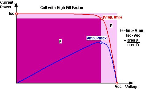
Now, we should know about the Fill-Factor. what is Fill Factor or FF
The fill f actor, more commonly known by its abbreviation FF, is a parameter which, in conjunction with the open circuit voltage and short circuit current of the panel, determines the maximum power from a solar cell. A solar micro-inverter in the process of being installed . The ground wire is attached to the lug and the panel's DC connections are attached to the cables on the lower right. The AC parallel trunk open circuit voltage and short circuit current of the panel, determines the maximum power from a solar cell. Fill f actor is def ined as the ratio of the maximum power f rom the solar cell to the product of Voc and Isc.
 There are three main types of MPPT algorithms: perturb-and-observe, incremental conductance and constant voltage. The first two methods are often referred to as hill climbing methods; they rely on the curve of power plotted against voltage rising to the left of the maximum power point, and falling on the right.

MPPT With FF Display

A general algorithm of MPPT shown here.


2.   Anti-Islanding Protection

In the event of a power failure on the grid, it is generally required that any grid-tie inverters attached to the grid turn off in a short period of time. This prevents the inverters from continuing to feed power into small sections of the grid, known as "islands". Powered islands present a risk to workers who may expect the area to be unpowered, but equally important is the issue that without a grid signal to synchronize to, the power output of the inverters may drift from the tolerances required by customer equipment connected within the island. 

Detecting the presence or lack of a grid source would appear to be simple, and in the case of a single inverter in any given possible physical island (between disconnects on the distribution lines f or instance) the chance that an inverter would f ail to notice the loss of the grid is effectively zero. However, if there are two inverters in a given island, things become considerably more complex. It is possible that the signal from one can be interpreted  as a grid feed from the other, and vice versa, so both units continue operation. As they track each other's output, the two can drift away from the limits imposed by the grid connections, say in voltage or frequency.

 There are a wide variety of methodologies used to detect an islanding condition. None of these are considered fool-proof , and utility companies continue to impose limits on the number and total power of solar power systems connected in any given area. However, many in-field tests have failed to uncover any real-world islanding issues, and the issue remains contentious within the industry.


3.    Redundancy

Redundancy is one of the main reason string inverters and microinverters are chosen instead of central inverters because in case of failure a smaller part of the system will be affected. String inverters have the added benefit of being a standard readily available commercial component which means it’s possible to let a local installer or facility manager exchange the inverter if necessary; also extra inverters can be kept in stock for quick exchange. Conversely, service contracts should be offered with central inverters and they should be serviced only by trained experts.

4.  Total Harmonic Distortion

The total harmonic distortion, or THD, of a signal is a measurement of the harmonic distortion present and is defined as the ratio of the sum of the powers of all harmonic components to the power of the fundamental frequency. THD is used to characterize the linearity of audio systems and the power quality of electric power systems.
So, it is desired that a inverter should have feature to cancel out the most of the higher harmonics as possible

.


When the input is a pure sine wave, the measurement is most commonly the ratio of the sum of the powers of all higher harmonic frequencies to the power at the first harmonic, or fundamental, frequency.
 \mbox{THD} = \frac{P_2 + P_3 + P_4 + \cdots + P_\infty}{P_1} = \frac{\displaystyle\sum_{i=2}^\infty P_i}{P_1}
which can equivalently be written as
 \mbox{THD} =  \frac{P_\mathrm{total} - P_1}{P_1}
if there is no source of power other than the signal and its harmonics.
Measurements based on amplitudes (e.g. voltage or current) must be converted to powers to make addition of harmonics distortion meaningful. For a voltage signal, for example, the ratio of the squares of the RMS voltages is equivalent to the power ratio:
 \mbox{THD} =  \frac{V_2^2 + V_3^2 + V_4^2 + \cdots + V_\infty^2}{V_1^2}
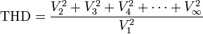
where Vi is the RMS voltage of ith harmonic and i = 1 is the fundamental frequency.
THD is also commonly defined as an amplitude ratio rather than a power ratio,[3] resulting in a definition of THD which is the square root of that given above:
 \mbox{THD} = \frac{ \sqrt{V_2^2 + V_3^2 + V_4^2 + \cdots + V_\infty^2} }{V_1}
This latter definition is commonly used in audio distortion (percentage THD) specifications. It is unfortunate that these two conflicting definitions of THD (one as a power ratio and the other as an amplitude ratio) are both in common usage.
So, it is desired that a inverter should have feature to cancel out the most of the higher harmonics as possible.


Follow me on Academia.edu
About the Author

Amrit Mandal is a final year B.tech (EE) Student, Admin of this blog. He likes to work in the renewable energy field-specially in solar energy field.
Follow Us on Twitter #REnergy_Blog

REnergy

Download