This is default featured slide 1 title

Lorem ipsum dolor sit amet, consectetur adipisicing elit, sed do eiusmod tempor incididunt ut labore et dolore magna aliqua. Ut enim ad minim veniam. blogger theme by BTemplates4u.com.

This is default featured slide 2 title

Lorem ipsum dolor sit amet, consectetur adipisicing elit, sed do eiusmod tempor incididunt ut labore et dolore magna aliqua. Ut enim ad minim veniam. blogger theme by BTemplates4u.com.

This is default featured slide 3 title

Lorem ipsum dolor sit amet, consectetur adipisicing elit, sed do eiusmod tempor incididunt ut labore et dolore magna aliqua. Ut enim ad minim veniam. blogger theme by BTemplates4u.com.

This is default featured slide 4 title

Lorem ipsum dolor sit amet, consectetur adipisicing elit, sed do eiusmod tempor incididunt ut labore et dolore magna aliqua. Ut enim ad minim veniam. blogger theme by BTemplates4u.com.

This is default featured slide 5 title

Lorem ipsum dolor sit amet, consectetur adipisicing elit, sed do eiusmod tempor incididunt ut labore et dolore magna aliqua. Ut enim ad minim veniam. blogger theme by BTemplates4u.com.

Saturday, 27 April 2013

Design Estimation of 5KWp Solar BIPV power system (Grid-tie)

this post is about a paper i made on designing and estimating the components and the various parameters required to set-up a 5KWp Building Integrated Photo-Voltaic Solar power system(grid-tie). I took our college buliding as a location because of simplification of the calculation. I included the detailed report on this paper here.kindly read it and post your feedback.
thank you


Follow me on Academia.edu
About the Author

Amrit Mandal is a final year B.tech (EE) Student, Admin of this blog. He likes to work in the renewable energy field-specially in solar energy field.
Follow Us on Twitter #REnergy_Blog

REnergy

Future wire ''NANOWIRE''

A nanowire is a nanostructure, with the diameter of the order of a nanometer (10−9 meters). Alternatively, nanowires can be defined as structures that have a thickness or diameter constrained to tens of nanometers or less and an unconstrained length. At these scales, quantum mechanical effects are important — which coined the term "quantum wires".

Many different types of nanowires exist, including metallic (e.g., Ni, Pt, Au), semiconducting (e.g., Si, InP, GaN, etc.), and insulating (e.g., SiO2, TiO2). Molecular nanowires are composed of repeating molecular units either organic (e.g. DNA) or inorganic (e.g. Mo6S9-xIx).

The nanowires could be used, in the near future, to link tiny components into extremely small circuits. Using nanotechnology, such components could be created out of chemical compounds.

Synthesis of nanowires

There are two basic approaches to synthesizing nanowires: top-down and bottom-up. A top-down approach reduces a large piece of material to small pieces, by various means such as lithography or electrophoresis. A bottom-up approach synthesizes the nanowire by combining constituent adatoms. Most synthesis techniques use a bottom-up approach.
Nanowire production uses several common laboratory techniques, including suspension, electrochemical deposition, vapor deposition, and VLS growth. Ion track technology enables growing homogeneous and segmented nanowires down to 8 nm diameter.

Suspension

A suspended nanowire is a wire produced in a high-vacuum chamber held at the longitudinal extremities. Suspended nanowires can be produced by:
  • The chemical etching of a larger wire
  • The bombardment of a larger wire, typically with highly energetic ions
  • Indenting the tip of a STM in the surface of a metal near its melting point, and then retracting it

VLS Growth

A common technique for creating a nanowire is Vapor-Liquid-Solid (VLS) synthesis. This process can produce crystalline nanowires of some semiconductor materials. It uses as source material either laser ablated particles or a feed gas such as silane.
VLS synthesis requires a catalyst. For nanowires, the best catalysts are liquid metal (such as gold) nanoclusters, which can either be self-assembled from a thin film by dewetting, or purchased in colloidal form and deposited on a substrate.
The source enters these nanoclusters and begins to saturate them. On reaching supersaturation, the source solidifies and grows outward from the nanocluster. Simply turning off the source can adjust the final length of the nanowire. Switching sources while still in the growth phase can create compound nanowires with super-lattices of alternating materials.
A single-step vapour phase reaction at elevated temperature synthesises inorganic nanowires such as Mo6S9-xIx. From another point of view, such nanowires are cluster polymers.

Uses of nanowires

Nanowires still belong to the experimental world of laboratories. However, they may complement or replace carbon nanotubes in some applications. Some early experiments have shown how they can be used to build the next generation of computing devices.
To create active electronic elements, the first key step was to chemically dope a semiconductor nanowire. This has already been done to individual nanowires to create p-type and n-type semiconductors.

The Future 

The next step was to find a way to create a p-n junction, one of the simplest electronic devices.

After p-n junctions were built with nanowires, the next logical step was to build logic gates. By connecting several p-n junctions together, researchers have been able to create the basis of all logic circuits: the AND, OR, and NOT gates have all been built from semiconductor nanowire crossings.


Follow me on Academia.edu
About the Author

Amrit Mandal is a final year B.tech (EE) Student, Admin of this blog. He likes to work in the renewable energy field-specially in solar energy field.
Follow Us on Twitter #REnergy_Blog

REnergy

Friday, 26 April 2013

Lead-Acid Battery charger circuit

In this article i'm going to discuss about a lead-acid battery chrager construction and a very basic principle of charging ckt. Also i'll share my own battery charger that i've built to use my project.


Brief Description
Input of this prototype is 12v,1amp DC power supply.using a voltage regulator IC, a comparator IC and a Double transistor package module the circuit gives output of 6v DC.  A 6v, 5Ah lead-acid battery can be charged using this circuit.

Circuit Design:


LM 317


Components Used:
ICs:
a) LM 317 (v-reg) - 1
b) IC 741 (comparator) - 1
c) TIP 122 (transistors) - 1
Resistors:(all are 1/4 watts)
470 ohms: 1
220 ohms: 1
100 ohms: 1
10k ohms: 1
1k   ohms: 1
100kohms:1
2k2 preset pot:1
10k preset pot:1
Diodes:
1N4007 : 2
3.3v Zener : 2
0.1uF capacitor : 1(disk type)
LED: green & red : one each


IC 741


Testing of the Circuit
1)    The input to the circuit can be fed from a standard 12V 1 amp adapter.

2)    To set up the circuit initially do not connect any battery.

3)    Feed 12V input, adjust the 2K2 pot to get 7v across the battery charging terminals.

4)    Next, adjust the 10K preset such that the green LED just lights up fully and the red LED shuts off.

5)    Circuit has been set.

6)    Switch OFF power. Connect a discharged battery and switch ON power, the circuit will do the rest.it will cut off as as soon as the battery voltage reaches 7V.


The prototype model i've built:

 1. this is the circuit set-up in 3.5x6 inches box. Input of this circuit comes from two 6v, 3watt solar modules connected in series to get 12v,1amp DC output.

2. the output of the circuit is connected to a 6v,5Ah lead-acid battery which is fully charged.
that' why the RED LED is lighted up.
3. you can see the multi-meter reading.
It shows that the battery-voltage is 6.36v. and because of that the RED LED is blinking.

Sensitive Smart Skin : New Technology

An array of piezotronic transistors capable of converting
mechanical motion directly into electronic controlling signals
Knitting  zinc oxide nano-wires vertically, researchers of Georgia Institute of Technology have fabricated arrays of piezoelectric transistors which are capable of converting mechanical motion directly into electronic controlling signals.It can sense touch with the same level of sensitivity as the human fingertip, which could result in better bots and prosthetic.


"Any mechanical motion, such as the movement of arms or the fingers of a robot, could be translated to control signals," lead author Zhong Lin Wang of Georgia Tech's School of Materials Science and Engineering said in a news release. "This could make artificial skin smarter and more like the human skin. It would allow the skin to feel activity on the surface."
The transparent and flexible arrays use about 8,000 taxels. A taxel is a touch-sensitive transistor that can generate piezoelectric signals independently, i.e., emit electricity when mechanically agitated. Each of those two-terminal transistors are constructed with 1,500 zinc oxide nano-wires(500-600 nanometers in diameter). In the array the vertical piezotronic transistors are placed between top and bottom electrodes which are made of indium tin oxide aligned in orthogonal cross-bar configurations. A thin layer of gold is deposited between the top and bottom surfaces of the zinc oxide nano-wires and the top and bottom electrodes, forming Schottky contacts. A thin layer of the polymer Parylene is then coated onto the device as a moisture and corrosion barrier.The array density is 234 pixels per inch, the resolution is better than 100 microns, and the sensors are capable of detecting pressure changes as low as 10 kilo-pascals (resolution comparable to that of the human skin), Wang said. The Georgia Tech researchers fabricated several hundred of the arrays during a research project that lasted nearly three years.
Figure shows a scanning electron microscopy image (A) and topological profile image of fabricated strain-gated piezotronic transistor array. An optical image shows (B) the transparent and flexible SGPT array on flexible substrate


The arrays are fabricated on flexible substrates
In the laboratory, the research group has fabricated arrays of 92 X 92 transistors. The researchers used a chemical growth technique at approximately 85 to 90 degrees Celsius, which allowed them to fabricate arrays of strain-gated vertical piezotronic transistors on substrates that are suitable for microelectronics applications.
 The research group measured the tiny polarization changes when piezoelectric materials such as zinc oxide are placed under mechanical stress. Zinc oxide is used because it can accumulate current. In those transistors, then piezoelectric charges control the flow of current through the nano-wires.Passing the control is known as  “strain-gating.” The technique only works in materials that have both piezoelectric and semiconducting properties. These properties are seen in nano-wires and thin films created from the wurtzite and zinc blend families of materials, which includes zinc oxide, gallium nitride and cadmium sulfide.
The arrays could help give robots a more adaptive sense of touch, provide better security in handwritten signatures and offer new ways for humans to interact with electronic devices. "This is a fundamentally new technology that allows us to control electronic devices directly using mechanical agitation," Prof Wang said. "This could be used in a broad range of areas, including robotics, MEMS, human-computer interfaces, and other areas that involve mechanical deformation."


 Potential Applications:

  •     Multidimensional signature recording, in which not only the graphics of the signature would be included, but also the pressure exerted at each location during the creation of the signature, and the speed at which the signature is created.
  •     Shape-adaptive sensing in which a change in the shape of the device is measured. This would be useful in applications such as artificial/prosthetic skin, smart biomedical treatments and intelligent robotics in which the arrays would sense what was in contact with them.
  •     Active tactile sensing in which the physiological operations of mechanoreceptors of biological entities such as hair follicles or the hairs in the cochlea are emulated.


Future work will include producing the taxel arrays from single nano-wires instead of bundles, and integrating the arrays onto CMOS silicon devices. Using single wires could improve the sensitivity of the arrays by at least three orders of magnitude, Wang said.
The research was reported April 25, 2013 in the Journal Science online and will be published in a later version of the print journal. The research has been sponsored by the Defense Advanced Research Projects Agency (DARPA), the National Science Foundation (NSF), the U.S. Air Force (USAF), the U.S. Department of Energy (DOE) and the Knowledge Innovation Program of the Chinese Academy of Sciences.


Follow me on Academia.edu
About the Author

Amrit Mandal is a final year B.tech (EE) Student, Admin of this blog. He likes to work in the renewable energy field-specially in solar energy field.
Follow Us on Twitter #REnergy_Blog

REnergy

Internet Access Through LED bulb: Li-Fi

Imagine you are standing under a street light to get public internet access, or downloading a HD full movie from the lamp of your desk in  a few seconds, or posting your just clicked snap during a flight. No, I'm not talking about an upcoming Sci-Fi movie. There  is a newborn technology, which could meet the ever-increasing demand for high-speed wireless connectivity. Radio waves are replaced by light waves in a new method of data transmission which is being called Li-Fi.


Genesis

The technology Li-Fi was pioneered by German physicist Harald Haas, currently based at the University of Edinburgh in the UK. Haas coined the term Li-Fi in 2011 in the context of a talk presenting the new technology at the TED (Technology Entertainment and Design) Global conference. The word quickly entered common parlance as an instantly recognizable alternative to WiFi. Both terms are examples of abbreviations linguists sometimes describe as clipped forms, i.e. WiFi = wireless fidelity, Li-Fi = light fidelity. Haas's research project, originally known as D-Light (short for Data Light), is now set to launch a prototype Li-Fi application under the name of newly-formed company VLC (Visible Light Communication) Ltd, which was set up to commercialize the technology. 
Prof. Harald Haas, Edinburgh, Germany


According to researchers led by a team from the University of Strathclyde, it could be possible to combine domestic lighting to also illuminate homes with the technology, which claims to offer high-definition film downloads in under a minute. Professor Martin Dawson, of Strathclyde, who is leading the four-year initiative, said “Imagine an LED array beside a motorway helping to light the road, displaying the latest traffic updates and transmitting internet information wirelessly to passengers’ laptops, netbooks and smartphones. This is the kind of extraordinary, energy-saving parallelism that we believe our pioneering technology could deliver.”


How Li-Fi Works?

Li-Fi is typically implemented using white LED light bulbs at the downlink transmitter. These devices are normally used for illumination only by applying a constant current. However, by fast and subtle variations of the current, the optical output can be made to vary at extremely high speeds. This very property of optical current is used in Li-Fi setup. The operational procedure is very simple-, if the LED is on, you transmit a
digital 1, if it’s off you transmit a 0. The LEDs can be switched on and off very quickly, which gives nice opportunities for transmitting data. Hence all that is required is some LEDs and a controller that code data into those LEDs. All one has to do is to vary the rate at which the LED’s flicker depending upon the data we want to encode. Further enhancements can be made in this method, like using an array of LEDs for parallel data transmission, or using mixtures of red, green and blue LEDs to alter the light’s frequency with each frequency encoding a different data channel. Such advancements promise a theoretical speed of 10 Gbps – meaning one can download a full high-definition film in just 30 seconds.
 A novel modulation technique coined SIM-OFDM was recently proposed. SIM-OFDM uses different frequency carrier states to convey information and leads to increased performance in comparison to conventional OFDM. Additionally, its innovative structure can lead to a decrease of the peak system power, which is highly beneficial in the context of optical wireless communication.

Economic value

  • A free band that does not need license.
  • High installment cost but very low maintenance cost.
  • Cheaper than Wi-Fi.
  • Theoretical speed up to 1 GB per second : Less time & energy consumption.
  • No more monthly broadband bills.
  • Lower electricity costs.
  • Longevity of LED bulb : saves money.
  • Light doesn't penetrate through walls : secured access.

Limitations

The main problem is that light can't pass through objects, so if the receiver is inadvertently blocked in any way, then the signal will immediately cut out. "If the light signal is blocked, or when you need to use your device to send information -- you can seamlessly switch back over to radio waves", Harald says.
Reliability and network coverage are the major issues to be considered by the companies while providing VLC services. Interferences from external light sources like sun light, normal bulbs; and opaque materials in the path of transmission will cause interruption in the communication. High installation cost of the VLC systems can be complemented by large-scale implementation of VLC though Adopting VLC technology will reduce further operating costs like electricity charges, maintenance charges etc.

Future Prospects

This research report categorizes the global VLC technology market; based on component, applications, and geography. Li-Fi uses light-emitting diodes (LEDs) which are rapidly gaining in popularity for standard lightbulbs and other domestic and commercial purposes. They are expected to be ubiquitous in 20 years. VLC is not in competition with WiFi, Prof. Haas says, it is a complimentary technology that should eventually help free up much needed space within the radio wave spectrum.
"We still need Wi-Fi, we still need radio frequency cellular systems. You can't have a light bulb that provides data to a high-speed moving object or to provide data in a remote area where there are trees and walls and obstacles behind," he says.

some hotspots are:

  • the remote control devices under the ocean : radio wave doesn't work there.
  • petrochemical plants : radio wave data tranmission is not secured there.
  • hospitals : for medical purpose.
  • street lights, traffic signals : for traffic update.
    • aircraft cabins : for emmegency conversations.


    A power point slideshow on this topic provided here.Please give your valuable feedback.


      Thursday, 25 April 2013

      Wind Turbine Inspector::Helical Robotics

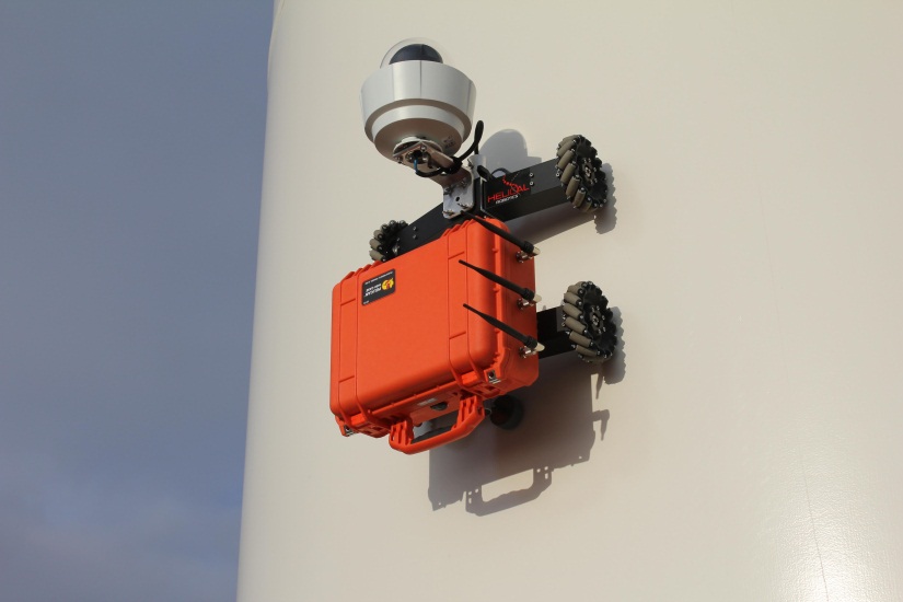
      How do you inspect the outside of a wind turbine? Either stand on the ground and use a telescope, or set up some climbing gear and scale the tower. The first solution is imprecise and the second is expensive and dangerous. Both are time-consuming. Now there's a third option: the HR-MP20 Light Weight Magnetic Climbing Robot by Helical Robotics.


       This remote-controlled robot can scale a turbine tower while carrying up to 9 kg (20 lbs) of inspection gear such as cameras and ultrasound. It clings to the tower using five neodymium magnets, the strongest type of permanent magnet available. A technician stands on the ground with a transmitter, directing the robotic inspector to various places on the turbine.


      The HR-MP20 features a zero turning radius and it can climb at a rate of 20 meters per minute (65 ft/min) and descend at 27 m/min (90 ft/min). It uses a 15 Ah lithium-polymer battery pack for its drive motors, a 10Ah NiMH battery pack to power its payload, and a 4.5Ah NiMH battery for its radio. The radio operates in the 2.4GHz band with a range of 762 m (2500 ft). Its size and capacity can be custom-engineered according to client needs. 

      Inspecting the blades of a wind turbine requires that the blades be stopped. Using the telescope method, a technician stands away from the turbine and looks at the blades through a telescope. This process can take up to four hours per turbine. Climbing a turbine requires a lot of rope, a strong technician, and a hefty insurance premium. Robotic inspection is faster, safer, less expensive, and more reliable than the telescope or climbing methods. Less down-time translates into more energy production. The HR-MP20 has been proven to work in high winds (which you're likely to find on a wind farm, right?) and bad weather, both of which will delay manual inspections. Of course, you still need a technician to climb up the inside of the tower to perform maintenance on the internal gears, generator, and other moving parts. But the towers have ladders on the inside, and wind is not a factor inside the tower. 
      Here it is action:

      Link to the original site : :Helical Robotics : HR-MP20 Magnetic Platform Lifting Vehicle


      Follow me on Academia.edu
      About the Author

      Amrit Mandal is a final year B.tech (EE) Student, Admin of this blog. He likes to work in the renewable energy field-specially in solar energy field.
      Follow Us on Twitter #REnergy_Blog

      REnergy

      Hydrogen Fuel Cell !!! New source of 'R'energy .


      This is the world’s first scalable Hydrogen-On-Demand process requiring minimum power input.

      An important characteristic of this new breakthrough is that it requires no external power input after the hydrogen-producing reaction is started, making possible, for the first time, the scale-up to high rates of hydrogen on demand (HOD) using water and scrap materials for fuel.


      A growing number of equipment manufacturers are planning the commercialization of this new low-cost, safe method for producing hydrogen fuel at high flow rates by extracting hydrogen from water, using scrap paper and scrap aluminum, two of the world’s safest and lowest-cost industrial materials. Phillips Company will use a worldwide central licensing agent to rapidly license this new technology.

      Experts agree that hydrogen will command a key role in future renewable energy. For years, the world’s clean-energy goal has been to have a relatively cheap, safe, efficient and non-polluting means of producing hydrogen on demand, at very high rates which make hydrogen storage tanks unnecessary. That goal has been met, for the first time, with a new process using safe, low-cost materials.

      Research resulted in the discovery that scrap aluminum and scrap paper, when burned, can be subjected to an inexpensive catalytic activation process. Then, this mixture can effectively generate hydrogen gas from water. The process uses more water than scrap materials, and the scrap materials do not have to be pure, making the fuel less expensive.

      The hydrogen production can operate in pH-neutral water, even if it is dirty, and can operate in sea water, the most abundant source of hydrogen on earth. The unique thing: This is the world’s first method that can produce more energy from the burning or combustion of hydrogen than the small amount of energy required to generate the hydrogen.

      Hydrogen is an energy dense and clean fuel, which upon combustion releases only water vapor. Today, most hydrogen is produced from thermoforming and electrolysis. Those methods require large amounts of electrical energy and/or result in excessive carbondioxide emissions. An alternative, clean method is to make hydrogen from water.

      The new process is called CC-HOD, or Catalytic Carbon, Hydrogen on Demand. Before this new process was developed, the use of hydrogen fuel was limited by the lack of a cheap catalyst that can speed up the generation of hydrogen from water. The new catalytic process is based on chemistry theory that is developed and ready for commercialization. “

      These applications are now possible because this process is the world’s first method that can be scaled up to produce hydrogen on demand at very high flow rates using catalytic carbon to limit the input energy to only a small amount. Because the hydrogen-producing process uses pH-neutral chemistry, the hardware corrosion problems are virtually nil.

      “Introduction of this new technology will first be used as a fuel supplement to increase the efficiency and reduce the cost of existing petroleum fuels. This can be done without modification to existing engines in any way apart from introducing the hydrogen into the air intake manifold of the engine. This has been demonstrated by using hydrogen as a fuel additive in conventional automobiles to increase the mileage (miles per gallon) by more than 30% with no modification to the engine,” said a company spokesman.

      Download